People who have worked in the fab
Lenspathio's team has a combined background spanning semiconductor equipment engineering, industrial computer vision, process integration, and algorithm development for sub-7nm nodes.
Leadership
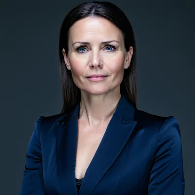
Diana Muller
Diana spent 12 years at semiconductor equipment companies before founding Lenspathio. She previously ran process integration for advanced logic at a 300mm fab, managing recipe qualification for 28nm and 16nm technology nodes. Her work at the equipment-fab interface gave her detailed visibility into the limitations of threshold-based defect classification. MS in Electrical Engineering from University of Michigan, with focus on optical sensing and measurement systems.
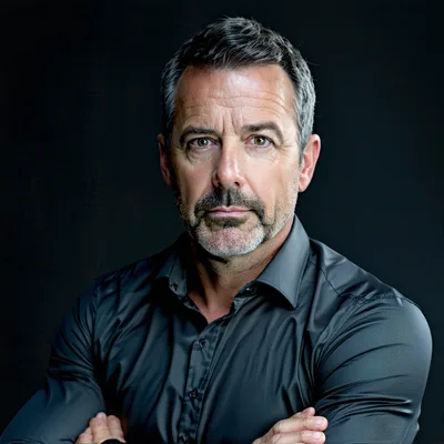
Marcus Holt
Marcus has a decade of experience developing convolutional neural network architectures for industrial inspection applications, including PCB defect detection and solar cell surface inspection before moving to semiconductor manufacturing. His research focused on model calibration for low false-positive industrial classifiers. PhD in Computer Vision from University of Colorado Boulder.
Technical team

Priya Nair
Leads development of the per-recipe adaptive calibration system. Background in statistical process control and real-time signal processing for semiconductor manufacturing equipment. Previously at a major inspection metrology OEM.
Leon Brauer
SECS/GEM protocol specialist. Wrote the HSMS-SS transport layer and GEM host interface. Extensive experience with MES/RTMS integration at 300mm logic and memory fabs. Previously at a semiconductor MES vendor.
Stefan Köhler
Develops and maintains the defect classification model architecture. Focus on model robustness across process node transitions and tool-to-tool transfer. Background in machine learning for semiconductor defect recognition. MS in Computer Vision from ETH Zürich.
Ryo Tanaka
On-site support lead for evaluation deployments. Handles recipe qualification, ATC qualification, and first-lot inspection reviews with fab process engineers. Background in defect reduction engineering at 300mm DRAM and NAND fabs.
Anika Moser
Responsible for inspection platform hardware integration, GPU compute cluster configuration, and camera/optics calibration. Background in precision machine vision systems for flat panel and semiconductor applications.
Kai Nakamura
Data pipeline and inspection result logging infrastructure. Builds the backend systems that handle inspection event streams, defect map storage, and KLARF/CSV export. Background in high-throughput data processing for industrial systems.
Work with us on an evaluation
Our process applications engineers travel to your facility for on-site deployment and qualification. Evaluations typically run 3–4 weeks.