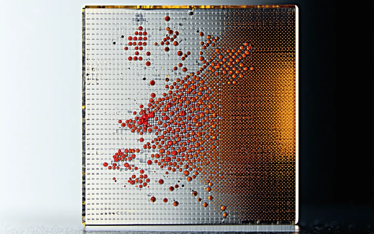
Computer Vision for Semiconductor QA
Wafer inspection at
production line speed.
False positives below 0.1%. 120 wafers per hour. Compatible with 3nm process nodes.
at production conditions
300mm scan mode
coverage validated
classified per inspection
The Problem
Third-shift decisions carry escape rates 3–4× higher than first shift
At 2 AM, the physics of attention defeat the most experienced QA operator. Lot disposition decisions made at hour 11 of a 12-hour shift produce escaped defect rates that don't appear in SPC charts — they show up in downstream electrical test yield, weeks later, after the process window has moved on.
A 2% false positive rate sounds manageable until you calculate the rework cost. At 120 wph throughput, 2% FPR means 2.4 wafers per hour sent back for re-inspection that are actually clean. That's roughly 14 wafers per shift on a continuous 300mm line — consuming tool time, operator attention, and lot cycle time with no yield benefit.
Technology
CNN architecture built for fab-native inspection
Four design principles separate production-grade computer vision from research-grade prototypes.
Optical-domain augmentation
Training data includes synthetic wafer defect images generated from optical physics models — calibrated to 193nm ArF and 13.5nm EUV illumination spectra — not generic natural-image augmentation pipelines.
Confidence-calibrated output
Every classification decision carries a calibrated confidence score. Die-level decisions below configurable thresholds are automatically escalated to human review — no silent misclassifications.
On-premises inference only
All model inference runs on validated on-premises hardware. No wafer image data leaves the fab network. Compatible with air-gapped environments and OEM-qualified hardware configurations.
SECS/GEM native output
Inspection results surface directly to your MES and APC systems via SECS/GEM II, GEM 300, and optionally KLARF-compatible output — no custom middleware required.
Coverage
Process node coverage matrix
Validated defect detection across six process nodes and five defect taxonomy categories.
Integration
SECS/GEM native — no custom middleware
Inspection results flow to MES, APC, and AMHS over validated SECS/GEM II and GEM 300 (SEMI E40/E87) interfaces — the same protocols your existing etch, CVD, and CMP tools already use. No API translation, no custom middleware, no additional equipment vendor qualification for the communication layer.
Chassis qualified to IEC 61000-6-2 industrial immunity. On-premises inference only — no outbound network calls. Wafer image data never leaves the fab network. Air-gap compatible.
- SECS/GEM II & GEM 300 (SEMI E40/E30) certified protocol stack
- KLARF-compatible defect file output for SEM review workflow compatibility
- On-premises inference: air-gap compatible, no cloud dependency
- OEM-qualified hardware: validated server configurations for fab-floor deployment
Results
What process engineers see
Our SEM review queue was saturated — we were spending more time on false-positive re-review than on actual defect analysis. After qualifying Lenspathio on our 7nm line, the number of wafers reaching SEM review dropped by roughly half. The ones that did reach review were genuinely worth reviewing.
Senior Yield Engineer
Logic foundry, 7nm production line
The E40 process job definition and E87 carrier handshake configuration took about three days. We'd budgeted two weeks. The KLARF output fields matched our existing SEM review recipe without any coordinate offset correction — that alone saved a week of integration work.
Process Integration Lead
Memory fab, 128L 3D NAND line
We were skeptical that a system trained on silicon wafers would hold its FPR spec on GaN-on-silicon substrates — the surface optical properties are entirely different. The evaluation run on our epitaxial lots held to spec. We use darkfield mode for epitaxial inspection and brightfield for post-etch steps, and both are inside the 0.1% FPR target.
QA Manager
Power semiconductor manufacturer, 150mm GaN line
Send us your wafer set.
Run a structured evaluation on your own wafer data. We accept 200mm/300mm lots, existing KLARF inspection files, or raw SEM imagery. Response within 2 business days. No obligation.