Platform
Three modules. One inspection pipeline.
Optical inspection hardware integration, deep learning defect classification, and SECS/GEM process integration — designed as a unified system, not bolted-together components.
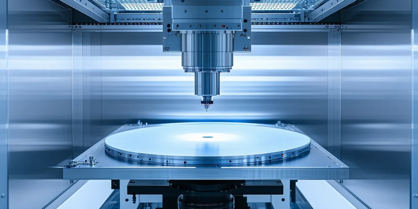
Wafer Inspection
Optical inspection at 120 wafers per hour. Supports 200mm and 300mm diameters. Multiple scan modes for brightfield, darkfield, and edge exclusion. Inline wafer map output at lot close.
Inspection specsDefect Classification
CNN-based taxonomy covering particles, scratches, crystal defects, edge exclusions, and pattern defects. Confidence scoring on every classification decision. Automatic escalation for below-threshold confidence.
Classification modelProcess Integration
SECS/GEM II and GEM 300 certified protocol stack. Direct MES/APC handshake. EMI-hardened enclosure. On-premises deployment with air-gap compatibility. Zero wafer data leaves the fab network.
Integration architectureDesigned for Fabs
Built from the fab floor up
Every design decision reflects the constraints of production semiconductor environments — not cloud-native assumptions imported into a manufacturing context.
On-premises only, by design
Fab IP stays in the fab. All inference runs on validated on-premises hardware. No telemetry, no model update pull from cloud. Compatible with full network isolation requirements.
EMI-hardened enclosure
Chassis and cabling designed to the IEC 61000-6-2 industrial immunity standard. Tested in high-RF-noise fab floor environments typical of RTP and etch equipment bays.
Human-review escalation loop
No silent misclassifications. Every die-level decision below the configurable confidence threshold routes to a human review queue — visible in the MES alongside the classification reason code.
Evaluation program first
Every engagement starts with a structured evaluation on your actual wafer data before any purchase decision. Send us your lot — or your existing KLARF files — and we run it through the full pipeline.
What Lenspathio is not
Lenspathio is a high-throughput optical inspection and classification layer — not a SEM review system, not a standalone metrology tool, and not a replacement for e-beam defect review. It is designed to be the first filter in the yield decision chain, flagging and classifying defects at lot close so that downstream SEM and metrology resources are directed at real yield risks, not false positives.
Start with your own wafer data.
Our evaluation program runs the full platform pipeline on your actual lot data. No obligation, no sales process before you see the numbers.